Share this
Our View On The SEMICON West 450MM Transition Forum
by Jeff Hopkins on 7/16/13 12:00 PM
As the industry gets ready for larger wafers, holding down costs through collaboration and innovation is the key to profitability

The 450mm Transition Forum emphasized that collaboration, innovation, and cost containment is critical to profitable success. We agree. We want to find innovative ways to collaborate with you Contact us »
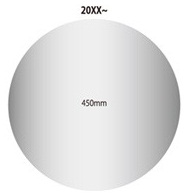
One highlight of this month's SEMICON West conference in San Francisco was a special forum on the pending industry transition to a larger silicon wafer, from 300 mm to 450mm. We were part of the standing-room-only audience, and were inspired by what we heard.
Jonathan Davis, global vice president of advocacy for SEMI, kicked it off by saying the upcoming transition is more than just adopting a larger wafer, it is an opportunity to transform the semiconductor industry through unprecedented collaboration and innovation.
He then introduced Paul Farrar, general manager of the Global 45MM Consortium, which we have written about in previous blog posts. His goal is to start high-volume manufacturing by 2015-2016 at the College of Nanoscale Science and Engineering fab in Albany, N.Y. He noted that there are currently eight new wafer tools installed and plans to bring in 10 tools per quarter. Wafer quality continues to improve, with the number of defects dropping by 90 percent since inception. It is now not a matter of if the transition will take place, but when. His team is already several weeks ahead of schedule. Farrar mentioned the importance of the newly formed Facility 450 Consortium, which includes Swagelok. This transformation is not just about 450mm wafers and 450 mm wafer tools, but about the facilities and supply chains that support it. That means Swagelok is part of a group that will be instrumental in this transformation.
Lessons learned
We also heard from Hamid Zarringhalam, executive vice president of Nikon Precision, who spoke about advanced lithography for 450mm application. Since 1974, the semiconductor industry has managed to reduce costs of a chip 30 percent per year, he said. This will be very difficult to continue in a 300mm environment, thus the push to 450mm. The new wafer increases the effective chip area by 2.4 times, which will stimulate greater economies of scale and foster tremendous industry innovation.
The industry also is looking at the lessons learned from the last transition. The development of the 300mm wafer cost nine times the previous transition to 200mm, and it took 14 years to recover the investment. The importance of the consortium is that we need unprecedented collaboration to minimize the cost of the transition to 450 mm. This collaboration would include: synchronized technology roadmaps, optimized timing, and risk and R&D cost sharing. The bottom line is that the transition must cost less than the productivity gained. Nikon will be providing 7500-8000 patterned 450mm wafers to the Global 450 Consortium by the end of 2014.
Holding down costs
Wrapping up the forum was Chris Richard, a partner at management consulting firm Pricewaterhouse Coopers, who outlined the profitability challenges faced in the 450mm transition. They include a smaller customer base, smaller production volumes, an uncertain adoption time, the complexity of scaling the old and new technologies simultaneously, and the need to keep investing in 300mm systems for now. But other industries have managed similar transitions well. He pointed to Boeing's transition from the 747 jetliner to the 777 and 787 over the past 30 years.
Richard outline three profitability opportunities:
- Standardize customer performance requirements. This would reduce the need for variable and customized configurations, and would mean simpler designs, production and maintenance. All those would hold down costs.
- Standardize select sub-systems and components where IP content is not critical to tool performance. This would reduce manufacturing complexity and the cost of inventory and servicing.
- Co-develop with suppliers. If suppliers are more involved in product development, each can focus on what it does best.
“The 450mm transition is raising significant profitability challenges for equipment vendors and suppliers. Other advanced manufacturing industries have leveraged similar transition to implement collaborative practice to enhance profitability," he said. "What will it take for the Semiconductor industry to the do the same?”
450 Panel
The presentation was followed by a lively panel discussion of leaders from four major equipment makers (Applied Material, Lam Research, KLA-Tencor, and Tokyo Electron Limited) that covered more than we can report here. But it re-enforced the notion that keeping down costs will be the key. To do this, the industry should expect more consolidation and drive more standardization, collaboration, and innovation. The final question to the panel asked them to predict how many 450mm high volume manufacturing lines will be in production by 2020, the consensus was four to five.
Additional resources
Downloads
Share this
- Archive (465)
- Assembly Services (207)
- About (100)
- Seal Support Systems (96)
- Best Practices (88)
- Training Services (74)
- Fittings (51)
- Semiconductor Applications (49)
- Hoses and Flexible Tubing (47)
- Regulators (44)
- Tubing (42)
- Grab Sampling Systems (32)
- Sampling Systems (32)
- Gas Systems (30)
- Services (30)
- Downloads (29)
- Valves (24)
- Application Support (18)
- Orbital Welding (17)
- Case Studies (13)
- Steam Systems (13)
- Frequently Asked Questions (12)
- Tools (12)
- Measurement Devices (7)
- Subsystems (6)
- Thermal Management (6)
- September 2023 (1)
- August 2023 (2)
- June 2023 (1)
- March 2023 (3)
- February 2023 (3)
- January 2023 (4)
- December 2022 (4)
- November 2022 (4)
- October 2022 (4)
- September 2022 (1)
- August 2022 (3)
- July 2022 (2)
- June 2022 (4)
- May 2022 (1)
- April 2022 (2)
- March 2022 (1)
- February 2022 (2)
- January 2022 (3)
- December 2021 (1)
- November 2021 (6)
- October 2021 (6)
- September 2021 (8)
- August 2021 (4)
- July 2021 (3)
- June 2021 (6)
- May 2021 (6)
- April 2021 (7)
- March 2021 (5)
- February 2021 (4)
- January 2021 (6)
- December 2020 (5)
- November 2020 (6)
- October 2020 (6)
- September 2020 (8)
- August 2020 (7)
- July 2020 (8)
- June 2020 (8)
- May 2020 (6)
- April 2020 (9)
- March 2020 (7)
- February 2020 (10)
- January 2020 (21)
- December 2019 (23)
- November 2019 (21)
- October 2019 (22)
- September 2019 (21)
- August 2019 (22)
- July 2019 (23)
- June 2019 (20)
- May 2019 (23)
- April 2019 (22)
- March 2019 (21)
- February 2019 (20)
- January 2019 (21)
- December 2018 (14)
- November 2018 (19)
- October 2018 (23)
- September 2018 (17)
- August 2018 (29)
- July 2018 (11)
- June 2018 (6)
- May 2018 (5)
- April 2018 (4)
- March 2018 (5)
- February 2018 (3)
- January 2018 (3)
- December 2017 (2)
- November 2017 (4)
- October 2017 (3)
- September 2017 (2)
- August 2017 (6)
- July 2017 (4)
- June 2017 (4)
- May 2017 (4)
- April 2017 (3)
- March 2017 (4)
- February 2017 (3)
- January 2017 (3)
- December 2016 (3)
- November 2016 (3)
- October 2016 (3)
- September 2016 (5)
- August 2016 (5)
- July 2016 (4)
- June 2016 (5)
- May 2016 (3)
- April 2016 (4)
- March 2016 (5)
- February 2016 (11)
- January 2016 (1)
- December 2015 (3)
- November 2015 (4)
- October 2015 (3)
- September 2015 (4)
- August 2015 (4)
- July 2015 (8)
- June 2015 (5)
- May 2015 (3)
- April 2015 (4)
- March 2015 (4)
- February 2015 (3)
- January 2015 (4)
- December 2014 (2)
- November 2014 (3)
- October 2014 (4)
- September 2014 (4)
- August 2014 (4)
- July 2014 (5)
- June 2014 (4)
- May 2014 (4)
- April 2014 (5)
- March 2014 (4)
- February 2014 (3)
- January 2014 (4)
- December 2013 (5)
- November 2013 (3)
- October 2013 (4)
- September 2013 (3)
- August 2013 (5)
- July 2013 (5)
- June 2013 (5)
- May 2013 (3)
- April 2013 (6)
- March 2013 (4)
- February 2013 (4)
- January 2013 (8)
- December 2012 (4)
- November 2012 (6)
- October 2012 (6)
- September 2012 (4)
- August 2012 (4)
- July 2012 (4)
- June 2012 (4)

.webp?width=210&height=70&name=StickyLogo%20(5).webp)
/ald,_dp,_df,_de1.jpg?width=250&height=178&name=ald,_dp,_df,_de1.jpg)
