
.webp?width=210&height=70&name=StickyLogo%20(5).webp "Swagelok Northern California home page")
Share this
by Morgan Zealear on 10/12/22 9:00 AM
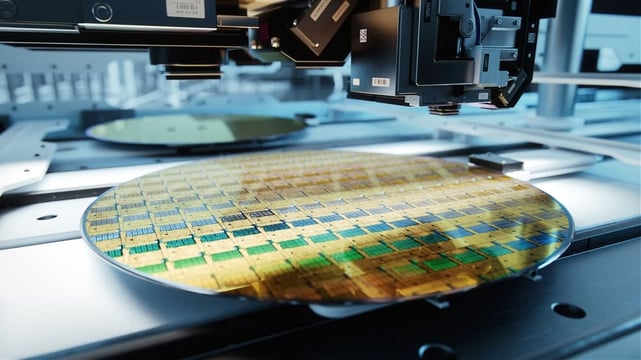
There are several techniques within semiconductor fabrication. These techniques allow semiconductor fabrication engineers to control temperature, apply layers with precision, remove degraded substances, and ionize chemicals in the semiconductor, among other processes. Fine control of the fabrication process is of the utmost importance to make a usable semiconductor free from contaminants. So to streamline production, many fabs in Northern California are looking to refine their techniques.
Refining semiconductor fabrication techniques involves maximizing the capabilities of semiconductor manufacturing equipment by ensuring it's assembled using only the highest quality components. High-quality components are designed to prevent thermal dissipation and leaks, and allow for precision control of techniques such as lithography, etching, and ionization.
Understanding Semiconductor Fabrication Techniques
Semiconductor fabrication involves several advanced techniques for precision layering and fabrication of semiconductors.
Deposition
Before fabrication, a silicon wafer must be polished to become extremely smooth. Polishing is often done with frozen argon, delivered by fluid system components. After polishing, thin conducting layers are deposited onto the semiconductor wafer. The more precise this process, the smaller and more advanced the semiconductor technology can become.
Photoresist Coating
The process of photoresist coating involves adding a light-sensitive coating over the wafer. When utilizing a positive resist coating, the areas coated will be chemically changed under ultraviolet light. When utilizing a negative resist coating, the areas under the coating will strengthen and will, ideally, not be affected by UV light. Both options allow for certain areas of the wafer to be ready for etching and deposition.
Photolithography
Photolithography involves placing the wafer into a machine where it's exposed to UV light. This light allows for extremely tiny and fine details to be ingrained into the chip. In this process, light is beamed onto the wafer into a prespecified pattern. This can be a complex and tricky process whereby many issues may cause the pattern to be incorrectly printed. One of the most common issues is particle interference distorting or blocking the printing from the UV light.
Etching
Etching involves removing degraded components to reveal the designated pattern. This is done by increasing temperature and pushing away unwanted substances through dry or wet etching. By using gases, dry etching will keep the pattern of the chip intact and remove unwanted particles. Similarly, wet etching uses liquid chemicals to wash the wafer and remove unwanted particles.
Ionization
By utilizing positive and negatively charged ions, the electrical conductivity of the semiconductor can be manipulated to the needed amount. Transistor gates are also created in this manner.
Packaging
The final chips need to be removed from wafers. Dozens to thousands of chips can be in one wafer. To remove the chips, a diamond saw is utilized. After the chip is removed from the wafer, it’s placed in a baseboard that uses metal foils to direct input and output signals. Finally, a heat spreader (a metal protective container with a cooling solution) works with a heatsink to make sure the microchip stays at the proper temperature during packaging.
Within each of these semiconductor fabrication techniques, there’s no room for error. Therefore, to limit excess waste and prevent damage to the final product, high-quality components must be used to assemble the equipment involved in each step.
Refining Semiconductor Fabrication Techniques with High-Quality Components
High-quality components can be used to refine semiconductor fabrication techniques by helping control the flow and pressure of gasses and liquids and the temperature for certain processes, and limiting contaminants from entering processes.
- Deposition and Layering Control: The deposition of layers on the chip needs to be precisely controlled. All components throughout the semiconductor fabrication process should ensure the correct quantity of substances is administered at the correct time. Leaks and failure to control temperature may affect the flow of substances.
- Lithography and Contaminant Prevention: Lithography can significantly damage chips if contaminants enter the system and block or refract UV light. Semiconductor fabrication equipment must be capable of preventing even the smallest contaminants from entering the process.
- Etching and Proper Gas and Fluid Distribution: The gasses and fluid used for etching need to be properly distributed to the correct location and in the correct quantities for processing to occur. The components that carry these gasses and fluids need to be reliable and safe from leakage.
- Etching and Temperature Control: The gases and liquid used for etching also need to be at the correct temperature and pressure throughout processing. The components of the semiconductor fabrication thus need to limit heat dissipation.
- Packaging and Temperature Control: The packaging of final chips involves keeping the semiconductor at the correct temperature using a heat spreader with the correct amount of cooling solution. It is imperative that the correct amount of cooling solution is present in the heat spreader.
To refine the semiconductor fabrication process, high-quality components should be used to control temperature, flow of substances, pressure of substances, and limit leaks and thermal dissipation. Swagelok has these components to help refine the semiconductor fabrication process.
Source High-Quality Components from Swagelok to Refine Semiconductor Fabrication Techniques
Swagelok Northern California has been serving the Bay Area (and surrounding areas) for more than 50 years. Our team of experts and high-quality components can help you streamline production by refining your semiconductor fabrication techniques. Our top-of-the-line equipment can provide exact thermal regulation during the production process to prevent heat dissipation that could lead to damaged semiconductors. Some of our solutions include:
- Insulated hoses, tubes, and lines: Insulated hoses, tubing, and lines absorb heat and prevent dissipation. By limiting heat dissipation, they prevent semiconductor damage. Having high-quality insulated hoses, tubes, and lines not only prevents direct damage to semiconductors but allows for more precise control of substances in the semiconductor fabrication process. Swagelok provides insulated options for temperatures ranging from -325°F to 1000°F (-200 to 537°C).
- Fittings and valves: Utilizing the proper fittings and valves will prevent contaminants from entering the semiconductor fabrication process. This is imperative in many steps in the process but particularly for lithography where contaminants will prevent the proper administering of UV light. In addition, improper fittings can result in leaks and poor temperature control. Swagelok’s fittings and valves will create the necessary fit to prevent such issues. We offer a catalog with multiple cleaning levels that meet industry standards.
- Measurement sensors: Measurement sensors must be able to detect small changes in temperature, flow, and pressure. Sensors may indicate that leaks are occurring or that machinery is not running properly. When issues arise, the real-time data collected by high-quality sensors can be quickly analyzed utilizing computer software and operators and maintenance personnel alerted to potential problems. Swagelok has high-quality sensors to quickly detect issues with temperature, flow, and pressure, that could be occurring during the semiconductor fabrication process.
Our team of experts is here to assist you with component selection and implementation to refine your semiconductor fabrication techniques. We provide expert, on-site consults to determine the exact configuration and components needed for cost-effective semiconductor fabrication. Because we’re a local provider of semiconductor components to Northern California, you quickly receive the components and ongoing support to streamline your process.
To find out more about how Swagelok Northern California can help you refine you semiconductor fabrication techniques with high-quality components, contact our team today by calling 510-933-6200.
 About Jason Burns| Technical Services Manager
Morgan holds a Bachelor of Science in mechanical engineering from University of California at Santa Barbara. He is certified in Section IX, Grab Sample Panel Configuration and Mechanical Efficiency Program Specification (API 682), and he is well versed in B31.3 Process Piping Code. Before joining Swagelok Northern, he was a manufacturing engineer at Sierra Instruments, primarily focused on capillary thermal meters for the semiconductor industry (ASML).