
.webp?width=210&height=70&name=StickyLogo%20(5).webp "Swagelok Northern California home page")
Share this
by Morgan Zealear on 10/18/22 9:00 AM
Much of the brains of modern technologies and innovations lie in the underlying component, specifically the semiconductor. With industries continuously working to develop smarter than before technologies, the demand for semiconductors is also showing an upward trend. The data for July 2022 alone shows global semiconductor sales worth 49 billion dollars, a growth of 7.3% from just a month prior.
To address these demands, it is important to understand the semiconductor fabrication process—from wafers to identifying the challenges that the production process may encounter. With Swagelok’s mission-critical components in place, wafer fabrication and semiconductor manufacturing processes can be reliable for semiconductors fabs in Northern California.
Wafer Fabrication and Challenges
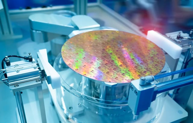
Semiconductor wafer fabrication can be considered to be the base process of any electronic device manufacturing. It starts with the retrieval and refining of the pure silicon crystals where the pre-designed electronic circuit is gradually deposited in layers. Once the photo masking is done for the layers and etching is performed to remove unwanted layers, the transistor gates and memory cells are added. Through metallic interconnection, the power transmission is established for these transistor gates following a similar process of deposition. The wafer fabricated through this rigorous process is then tested for quality and reliability.
The semiconductor wafer fabrication process requires extremely clean and Ultra High Purity conditions. This is the reason why most processes are conducted in controlled clean room environments. However, ensuring a high degree of cleanliness and safety is not the only challenge that semiconductor fabs face.
1. Temperature Control
Every step of the semiconductor wafer fabrication process is temperature controlled. For instance, photolithography has to be performed between 20°C to 30°C while dry etching is between -20°C to 80°C. Thin film deposition may require an even wider temperature range of -70°C to 200°C. The slightest error in this temperature margin can cause deposition or alignment errors.
Fluid is transferred through hoses or tubes to ensure the wafer doesn’t heat or cool excessively beyond the production temperature required. On the upper end, excessive heating of fluid can heat the wafer to a degree where it starts to bow. On the lower end of the temperature, fluids that have transitioned from their intended state can cause damage.
To ensure there is no loss of heat along the way, high-quality insulated components are required for minimal to no heat loss.
2. Gas Leaks
Semiconductor wafer processing requires the use of specialty gases at different steps such as deposition or etching. However, many of these gases can be of toxic and corrosive nature such as hydrogen sulfide, phosphine, diborane, or sulfur hexafluoride. In addition to being toxic, they are also flammable, so leaks put human lives at serious risk. The major cause of these leaks can be the use of components outside the required temperature and pressure range, as well as the poor attachment of the fittings and distribution system.
The solution is a gas distribution system that will help you significantly reduce leaks with its high-quality system components.
Improving Semiconductor Wafer Fabrication With Quality Solutions From Swagelok
Swagelok offers a wide range of thermal management solutions and gas distribution system components for semiconductor and wafer fabrication.
Thermal Management Solutions
The slightest temperature fluctuation can alter the properties of nanometric features on silicon wafers. Apart from the thermal expansion or contraction causing the alignment error, thermal fluctuation can also alter the conductivity of the wafer. The issues of lower throughput or failure of the semiconductors can be addressed with the installation of thermal management applications at the fabs.
Swagelok thermal management solutions include the use of jacketed tubings and vaporizing regulators to prevent heat loss and prevent condensation of the fluid media. Insulated tube options are available for a wide operating temperature range of -325°F to 1000°F (-200°C to 537°C).
Gas Distribution System
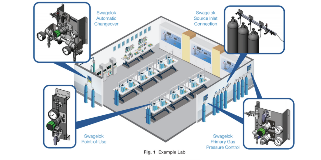
Swagelok can help you design the gas distribution system that will meet all the installation requirements for a safe and reliable supply of gas during wafer processing. The subsystem will include an inlet system, gas panels, a changeover system, and the point-of-use system.
The inlet system will usually have a gas manifold for safe delivery of the fluid into the distribution system. The gas panel is where the fluid pressure is regulated to reduce the build-up of pressure. In the changeover system, automatic switching between two gas tanks is made possible to ensure continuous system operation. The design of the point of use system will ensure pressure control at the point of consumption.
Design An Effective System At Your Semiconductor Fab
At Swagelok Northern California, our team of experts will help you analyze your current system and equipment and help you make the best decision. Our experts will not only guide you to the right equipment but will also help you in customizing the solutions to fit your production needs.
We also provide high-quality solutions such as gas panels and regulators so your distribution system can operate safely and efficiently. Our PVC-jacketed tubes and hoses, and valve systems will help you maintain the thermal efficiency of your controlled flow system. With expert advice and reliable components, you can improve the reliability of the semiconductor wafer fabrication process at your facility.
To find out more about how Swagelok Northern California can support your wafer fabrication and semiconductor assembly requirements, contact our team today by calling 510-933-6200.
 Morgan Zealear | Product Engineer – Assembly Services
Morgan holds a B.S. in Mechanical Engineering from the University of California at Santa Barbara. He is certified in Section IX, Grab Sample Panel Configuration, and Mechanical Efficiency Program Specification (API 682). He is also well-versed in B31.3 Process Piping Code. Before joining Swagelok Northern California, he was a Manufacturing Engineer at Sierra Instruments, primarily focused on capillary thermal meters for the semiconductor industry (ASML).